ycliper

Популярное

Музыка Кино и Анимация Автомобили Животные Спорт Путешествия Игры Юмор

Интересные видео

2025 Сериалы Трейлеры Новости Как сделать Видеоуроки Diy своими руками

Топ запросов

смотреть а4 schoolboy runaway турецкий сериал смотреть мультфильмы эдисон
Скачать

PCB Footprint Creation Made Easy (IPC Compliant Footprint Wizard)

Автор: Altium Academy

Загружено: 2022-09-01

Просмотров: 23630

Описание: 
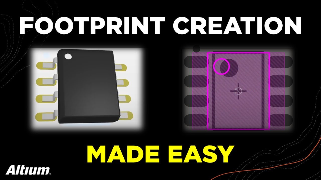
Footprint creation is typically a time-consuming, tedious, and error-prone process. Tech Consultant Philip Salmony from Phil's Lab outlines how Altium Designer's built-in 'IPC Compliant Footprint Wizard' can make footprint design simple and efficient, including automatic 3D model generation.

He explores an example footprint design for a SOIC-8 package, using the manufacturer's datasheet.

The IPC Compliant Footprint Wizard comes as part of Altium Designer and supports all standard footprint templates - from simple passive components to QFNs, BGAs, and more.

00:00 Introduction
00:46 IPC-7351 Standard
01:04 Example: SOIC-8
01:19 Datasheet Information
02:01 Footprint Library
02:17 IPC Compliant Footprint Wizard
04:08 Additional Parameters
05:56 Final Footprint
06:16 Outro

For more PCB Layout videos, click here:    • PCB Layout  
For more Tech Consultant Philip Salmony from Phil's Lab videos, click here:    • Tech Consultant Philip Salmony from Phil's...  
For more PCB Design for Beginnersvideos, click here:    • PCB Design for Beginners  

👉 15 Days Free Altium Designer Access: https://www.altium.com/yt/philslab

Don't forget to follow us on social to stay up-to-date on the latest Altium Academy content.
👉 Follow Altium on Twitter:   / altium  
👉 Follow Altium on Linkedin:   / altium  
👉 Follow Altium on Facebook:   / altiumofficial  


The Altium Academy is an online experience created to bring modern education to PCB Designers and Engineers all across the world. Here you can access a vast library of free training and educational content covering everything from basic design to advanced principles and step-by-step walkthroughs. Join industry legends as they share their career knowledge, review real-life design projects, or learn how to leverage one of Altium's leading design tools. No matter your level of experience, the Altium Academy can help you become a better Designer and Engineer!

About Altium LLC
Altium LLC (ASX:ALU), a global software company based in San Diego, California, is accelerating the pace of innovation through electronics. From individual inventors to multinational corporations, more PCB designers and engineers choose Altium software to design and realize electronics-based products.


#Altium #PCBdesign #AltiumDesigner

~-~~-~~~-~~-~
Check Out Our Latest Video: "How to Draw Antipads"
   • How to Draw Antipads - Complete Tutorial  
~-~~-~~~-~~-~

Не удается загрузить Youtube-плеер. Проверьте блокировку Youtube в вашей сети.
Повторяем попытку...
PCB Footprint Creation Made Easy (IPC Compliant Footprint Wizard)

Поделиться в:

Доступные форматы для скачивания:

Скачать видео

  • Информация по загрузке:

Скачать аудио

Похожие видео

QFN Layout and Routing - Tips & Tricks

QFN Layout and Routing - Tips & Tricks

Что не так со всеми слоями на печатной плате?

Что не так со всеми слоями на печатной плате?

Три инженера соревнуются в разработке печатной платы за 90 минут | Design Battle

Три инженера соревнуются в разработке печатной платы за 90 минут | Design Battle

Когда использовать отверстие в контактной площадке

Когда использовать отверстие в контактной площадке

Exploring Paste Mask & Solder Mask in Your PCB Footprint

Exploring Paste Mask & Solder Mask in Your PCB Footprint

Два инженера соревнуются в разработке печатной платы всего за час! Кто победит?

Два инженера соревнуются в разработке печатной платы всего за час! Кто победит?

8 - Create a Footprint for a QFN Package for ISL6236AIRZ

8 - Create a Footprint for a QFN Package for ISL6236AIRZ

Altium Designer RF Impedance Matching (e.g. 50Ω, USB, ...)

Altium Designer RF Impedance Matching (e.g. 50Ω, USB, ...)

Best CAD Software for 2026: TOP 9 CAD Tools Compared

Best CAD Software for 2026: TOP 9 CAD Tools Compared

Top 5 Beginner PCB Design Mistakes (and how to fix them)

Top 5 Beginner PCB Design Mistakes (and how to fix them)

(Sponsored) Symbol and Footprint Creation | Altium Designer - Phil's Lab #31

(Sponsored) Symbol and Footprint Creation | Altium Designer - Phil's Lab #31

🔥 DDR5 СВОИМИ РУКАМИ | Выживаем в кризис памяти 2026 года 💪| SODIMM - UDIMM без переходников

🔥 DDR5 СВОИМИ РУКАМИ | Выживаем в кризис памяти 2026 года 💪| SODIMM - UDIMM без переходников

То, что они только что построили, — нереально

То, что они только что построили, — нереально

Altium - Quick way to create symbols with many pins

Altium - Quick way to create symbols with many pins

How to Create IPC Compliant Footprint in OrCAD PCB Editor 17.4

How to Create IPC Compliant Footprint in OrCAD PCB Editor 17.4

Краткое руководство по Altium Designer от Фила Салмони из лаборатории Фила

Краткое руководство по Altium Designer от Фила Салмони из лаборатории Фила

Изготовление платы разработки ESP32 и создание собственной печатной платы за 3 шага.

Изготовление платы разработки ESP32 и создание собственной печатной платы за 3 шага.

KiCAD 9 tutorial course [06] - Footprint editor

KiCAD 9 tutorial course [06] - Footprint editor

Проектирование оборудования на базе микроконтроллера с помощью Altium Designer — №1 Введение и вы...

Проектирование оборудования на базе микроконтроллера с помощью Altium Designer — №1 Введение и вы...

Суперэффективное размещение компонентов печатной платы в Altium Designer

Суперэффективное размещение компонентов печатной платы в Altium Designer

© 2025 ycliper. Все права защищены.


  • Контакты
  • О нас
  • Политика конфиденциальности


Контакты для правообладателей: [email protected]