ycliper

Популярное

Музыка Кино и Анимация Автомобили Животные Спорт Путешествия Игры Юмор

Интересные видео

2025 Сериалы Трейлеры Новости Как сделать Видеоуроки Diy своими руками

Топ запросов

смотреть а4 schoolboy runaway турецкий сериал смотреть мультфильмы эдисон
Скачать

Imaging modes of AFM from the application point of view | Park Systems NanoAcademy

Автор: Park Systems

Загружено: 2021-07-15

Просмотров: 2720

Описание: 
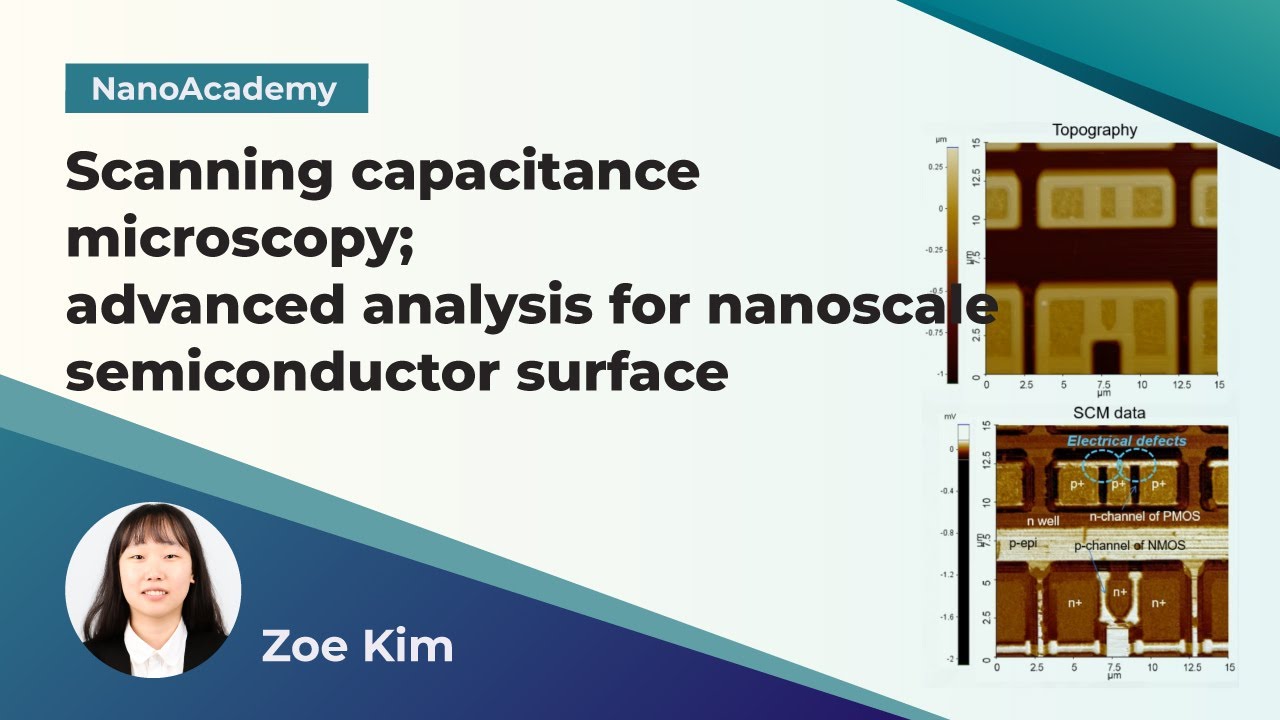
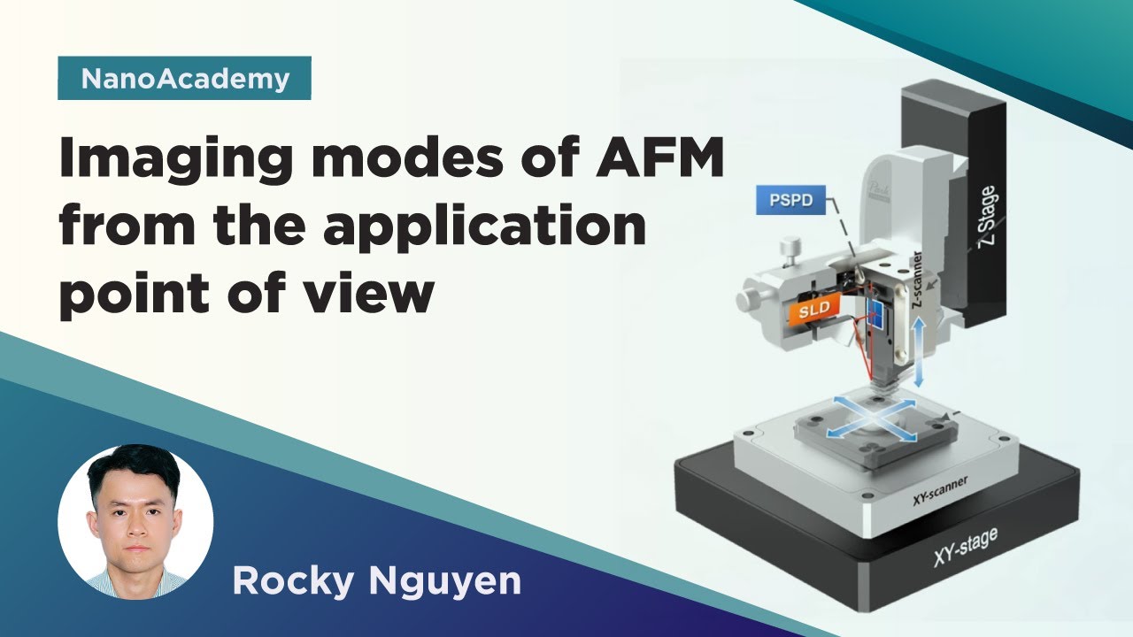
Understanding of surface structure and topography is essential for interpretation of material behavior at the nanoscale. To measure nano surfaces, different methods can be used such as confocal microscopy, scanning electron microscopy, transmission electron microscopy, and scanning probe microscopy (SPM). Atomic force microscopy (AFM) is a member in the SPM family that can measure various properties of samples in conjunction with their surface morphology. AFM allows quantitative measurement of surface features as small as angstrom level, which is relatively difficult to observe in conventional optical-based or electron beam-based techniques. To collect an AFM image, a sharp tip is typically used to sense the sample surface, and information on surface characteristics is accumulated by monitoring the tip-sample atomic interactions during scanning. Depending on specific applications, the AFM tip will come into direct contact (contact mode), intermittently contact (tapping mode), or scan over the sample surface at a given distance (non-contact mode). Contact, tapping, and non-contact are fundamental imaging modes of AFM. On the basics of these modes, various advanced techniques have been developed to measure different properties of samples such as electrical properties (C-AFM, KPFM, PFM modes, etc.), mechanical properties (nanoindentation, FD spectroscopy, and PinPoint modes), magnetic (MFM mode), and thermal (SThM mode) properties.

Within the scope of this webinar, practical applications of the imaging modes of AFM will be introduced. In addition, for better understanding on how AFM can measure your samples, a live session on imaging modes operations is also provided. It is expected that this webinar can be a useful material for gaining knowledge of AFM as well as its capabilities.

Presented By :
Rocky Nguyen, Park Systems Korea

Dr. Rocky Nguyen received his Ph.D. degree in Mechanical and Automotive Engineering from the University of Ulsan in South Korea and his Bachelor’s degree in Materials Engineering from Back Khoa University in Vietnam. He is currently focused on the development and performance optimization of atomic force microscopy and related techniques at Park Systems Korea.

#ParkSystems #AFMwebinar #AtomicForceMicroscopy

Не удается загрузить Youtube-плеер. Проверьте блокировку Youtube в вашей сети.
Повторяем попытку...
Imaging modes of AFM from the application point of view | Park Systems NanoAcademy

Поделиться в:

Доступные форматы для скачивания:

Скачать видео

  • Информация по загрузке:

Скачать аудио

Похожие видео

Sideband Kelvin Probe Force Microscopy for Advanced Materials Characterization | Park Webinar

Sideband Kelvin Probe Force Microscopy for Advanced Materials Characterization | Park Webinar

1,000,000x Magnification with Atomic Force Microscope

1,000,000x Magnification with Atomic Force Microscope

Nanomaterials Webinar : Nanostructured and Functional Templated Coatings

Nanomaterials Webinar : Nanostructured and Functional Templated Coatings

Bruker Atomic Force Microscope

Bruker Atomic Force Microscope

Как производятся микрочипы? 🖥️🛠️ Этапы производства процессоров

Как производятся микрочипы? 🖥️🛠️ Этапы производства процессоров

Investigation of nanomechanical properties using AFM | Park Systems Webinar

Investigation of nanomechanical properties using AFM | Park Systems Webinar

Но что такое нейронная сеть? | Глава 1. Глубокое обучение

Но что такое нейронная сеть? | Глава 1. Глубокое обучение

Визуализация гравитации

Визуализация гравитации

Demo: Imaging 2D Materials with the FlexAFM

Demo: Imaging 2D Materials with the FlexAFM

Observation of resistive switching at the nanoscale via conductive atomic force microscopy

Observation of resistive switching at the nanoscale via conductive atomic force microscopy

Парадокс разгибания кривой доски

Парадокс разгибания кривой доски

Introduction to the principle of an AFM | Park Systems Webinar

Introduction to the principle of an AFM | Park Systems Webinar

Минералы и их свойства. Как определить?

Минералы и их свойства. Как определить?

Bruker AFM: Driving Test SOP

Bruker AFM: Driving Test SOP

Что происходит с нейросетью во время обучения?

Что происходит с нейросетью во время обучения?

Scanning capacitance microscopy; advanced analysis for nanoscale semiconductor surface | NanoAcademy

Scanning capacitance microscopy; advanced analysis for nanoscale semiconductor surface | NanoAcademy

MS: P-11 Characterization techniques for materials II(e-PGP)

MS: P-11 Characterization techniques for materials II(e-PGP)

Live Demo | A Comparative Study for Surface Potential Mapping Using KPFM | Charles Kim | 2020NSSC

Live Demo | A Comparative Study for Surface Potential Mapping Using KPFM | Charles Kim | 2020NSSC

Как элементы приобретают свои физические свойства — простое объяснение | Арвин Эш

Как элементы приобретают свои физические свойства — простое объяснение | Арвин Эш

Atomic Force Microscopy (AFM)

Atomic Force Microscopy (AFM)

© 2025 ycliper. Все права защищены.


  • Контакты
  • О нас
  • Политика конфиденциальности


Контакты для правообладателей: [email protected]