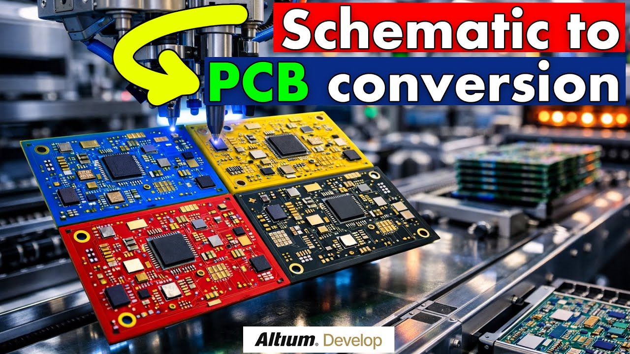
Schematic ➜ PCB Design Explained | Altium Designer Develop Tutorial
Автор: Engineering Science & Technology - EST
Загружено: 2025-12-25
Просмотров: 683
Описание:
Schematic ➜ PCB Design Explained | Altium Designer Developer Tutorial
🔥🔥🔥Altium Develop: http://altium.com/yt/engineeringscien...
Want to learn how to convert schematic design to PCB layout professionally?
In this video, you’ll learn the complete schematic to PCB design conversion process in Altium Designer Developer, explained step by step for beginners and professionals.
This tutorial covers real-world PCB design workflow used in industry — from schematic capture to final PCB board layout.
🔥Reference:
https://drive.google.com/drive/folder...
🔥 In This Video You Will Learn:
✔ How to prepare schematic for PCB design
✔ How to generate PCB from schematic (ECO)
✔ Understanding netlist & connectivity
✔ PCB rules setup (clearance, width, via)
✔ Component placement strategy
✔ Manual routing vs auto routing
✔ Design Rule Check (DRC) & error fixing
✔ Professional PCB finishing tips
This video is perfect for electronics students, PCB designers, Arduino users, and DIY creators who want to design error-free, professional PCB boards using Altium Designer.
📌 Watch till the end to avoid common PCB design mistakes that beginners usually
How to Convert Schematic into PCB Layout in Altium Designer ❓ COMPLETE GUIDE
👍 If you found this video valuable, give it a thumbs up. If you have questions or want to share your thoughts, feel free to leave a comment. Don't forget to hit that bell icon to receive notifications whenever we release new content.
📣Business Inquiry Mail: [email protected]
📌📌📌More Projects Videos:
• All-in-One Variable Power Supply ⚡🔋💡 Makin...
• Best IOT Project Making At Home using Micr...
• DIY Walking Robot Making at Home | Step-by...
• Universal Battery AutoCut Charge Controlle...
• Microcontroller Master Trainer Making At H...
• NOTHING Type POWER BANK Making At Home | P...
• Wireless Electricity Transformation || DIY...
• DIY DC Motor Speed Controller | Easy Step-...
• DIY Rechargeable Fan Making At Home || 5-6...
• DIY RGB Desk Fan with Adjustable Speed Con...
• এসি/ডিসি মিনি আইপিএস তৈরি ১৮৬৫০ ব্যাটারি প...
• 🔋 DIY 8-10Hr Backup UPS Making At Home | 1...
📊 Stay informed and updated on the latest tech trends. Subscribe now for more engaging content and expert tutorials! 🚀
📣 Follow us on social media for behind-the-scenes insights and more:
📘 Facebook Page: / engineering.science.2014
👥 Facebook Group: / engineeringsciencetechnology
📷 Instagram: / estiakhanjhuman
schematic to pcb design
schematic to pcb conversion
altium designer schematic to pcb
altium designer pcb tutorial
pcb design workflow
pcb layout design tutorial
how to convert schematic to pcb
altium designer developer
pcb routing tutorial
pcb design for beginners
professional pcb design
electronics pcb designing
altium eco process
manual routing vs autorouting
pcb design rules
est experiments
jhuman khan
#schematictopcb
#altiumdesigner
#pcbdesign
#electronics
#pcblayout
#altiumtutorial
Повторяем попытку...
Доступные форматы для скачивания:
Скачать видео
-
Информация по загрузке:


