ycliper

Популярное

Музыка Кино и Анимация Автомобили Животные Спорт Путешествия Игры Юмор

Интересные видео

2025 Сериалы Трейлеры Новости Как сделать Видеоуроки Diy своими руками

Топ запросов

смотреть а4 schoolboy runaway турецкий сериал смотреть мультфильмы эдисон
Скачать

How Nano Patterns Are Made? Building Electronic Chips

Автор: Quantum Leap

Загружено: 2024-12-04

Просмотров: 40313

Описание: The photolithography process is a cornerstone of modern CPU production. It begins with a silicon wafer, a thin slice of pure silicon that serves as the foundation. A light-sensitive material called photoresist is applied to the wafer, coating it evenly.

Using a precise optical system, ultraviolet light shines through a photomask—a stencil-like pattern representing the circuit design—onto the photoresist. The light alters the chemical properties of the photoresist in the exposed areas, making them soluble for removal in the next step. This process etches intricate patterns onto the wafer.

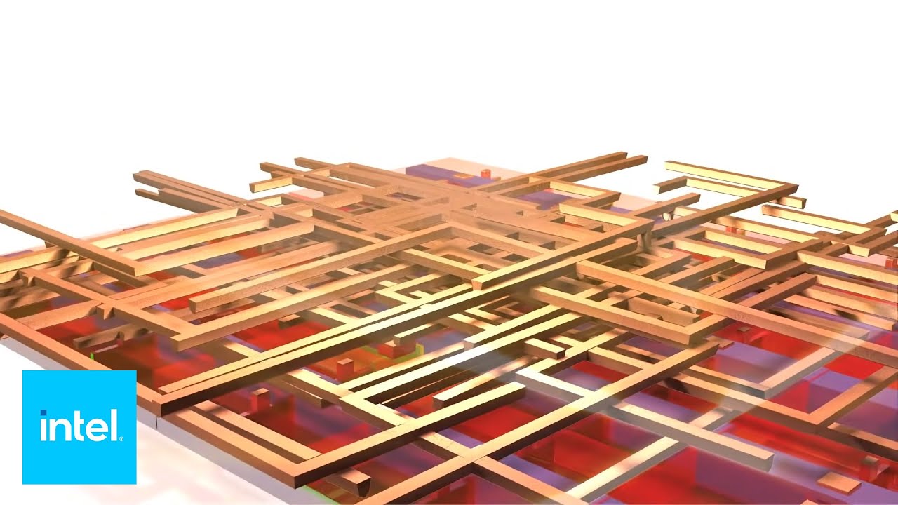
These patterns form the blueprint for the transistors and circuits that make up a CPU. Layer by layer, with different photomasks and materials, the process is repeated, creating complex 3D structures. Finally, the patterned wafer is baked, polished, and processed further, eventually becoming the brain of your computer. Photolithography is where precision meets innovation, enabling the incredible computing power we rely on every day.


Ref:

   • How are Microchips Made? 🖥️🛠️ CPU Manufact...  
   • Computational lithography: Driving nanomet...  

Не удается загрузить Youtube-плеер. Проверьте блокировку Youtube в вашей сети.
Повторяем попытку...
How Nano Patterns Are Made? Building Electronic Chips

Поделиться в:

Доступные форматы для скачивания:

Скачать видео

  • Информация по загрузке:

Скачать аудио

Похожие видео

How are BILLIONS of MICROCHIPS made from SAND? | How are SILICON WAFERS made?

How are BILLIONS of MICROCHIPS made from SAND? | How are SILICON WAFERS made?

Photolithography: Step by step

Photolithography: Step by step

Металлизация: создание токопроводящих дорожек на кремниевых чипах.

Металлизация: создание токопроводящих дорожек на кремниевых чипах.

"Z2" - Upgraded Homemade Silicon Chips

Как производятся микрочипы? 🖥️🛠️ Этапы производства процессоров

Как производятся микрочипы? 🖥️🛠️ Этапы производства процессоров

Speedrunning 30yrs of lithography technology

Speedrunning 30yrs of lithography technology

DIY Semiconductor Fabrication

DIY Semiconductor Fabrication

Nanoimprint Lithography (Canon Official)

Nanoimprint Lithography (Canon Official)

Intel: The Making of a Chip with 22nm/3D Transistors | Intel

Intel: The Making of a Chip with 22nm/3D Transistors | Intel

The Lithography Wars: The Story of How Nikon Lost to ASML

The Lithography Wars: The Story of How Nikon Lost to ASML

How are microchips made? - George Zaidan and Sajan Saini

How are microchips made? - George Zaidan and Sajan Saini

Раскрывая тайны кремния: разоблачение того, как создаются и работают чипы

Раскрывая тайны кремния: разоблачение того, как создаются и работают чипы

Что происходит с таблицей Менделеева на ячейке 137?

Что происходит с таблицей Менделеева на ячейке 137?

Как сделать процессор

Как сделать процессор

Electron Beam Lithography

Electron Beam Lithography

Fabrication Processes of a Chip: Photolithography

Fabrication Processes of a Chip: Photolithography

A Deep Dive Into Canon’s Nanoimprint Lithography

A Deep Dive Into Canon’s Nanoimprint Lithography

Gate-All-Around, Transistor Architecture Designed for the Future of Logic Devices (Semi 101)

Gate-All-Around, Transistor Architecture Designed for the Future of Logic Devices (Semi 101)

Топ-15 технологий, которые перевернут 2027 год

Топ-15 технологий, которые перевернут 2027 год

Maskless Photolithography Stepper for Homemade Chips

Maskless Photolithography Stepper for Homemade Chips

© 2025 ycliper. Все права защищены.


  • Контакты
  • О нас
  • Политика конфиденциальности


Контакты для правообладателей: [email protected]