PCB Design Basics: From Schematic to Final Layout
Автор: Gighz Technologies
Загружено: 2025-09-30
Просмотров: 7
Описание:
PCB design is the backbone of every electronic device. A well-designed PCB ensures performance, reliability, and manufacturability.
In this video, we cover:
What is PCB Design? Understanding the purpose and process ⚡
Key Steps:
Schematic Design & Netlists 📝
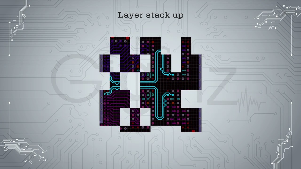
Layer Stack-Up: Single, Double, Multi-layer 🔄
Component Placement & Grouping 🛠️
Routing Traces: Manual vs Auto & Rules to Follow 🔗
Design Rule Check (DRC) ✅
Best Practices: Minimizing crosstalk, thermal management, ground & power planes
Popular Tools: Altium Designer, KiCad, Eagle, Cadence, Mentor Graphics 💻
Whether you’re a beginner or brushing up your skills, this guide will help you design PCBs efficiently and reliably.
#pcbdesign #electronicsdesign #cadencedesignsystems #pcblayout #eda
Повторяем попытку...
Доступные форматы для скачивания:
Скачать видео
-
Информация по загрузке: