Professional Inhouse PCB Multilayer Process
Автор: LPKF Laser & Electronics North America
Загружено: 2024-10-22
Просмотров: 1421
Описание:
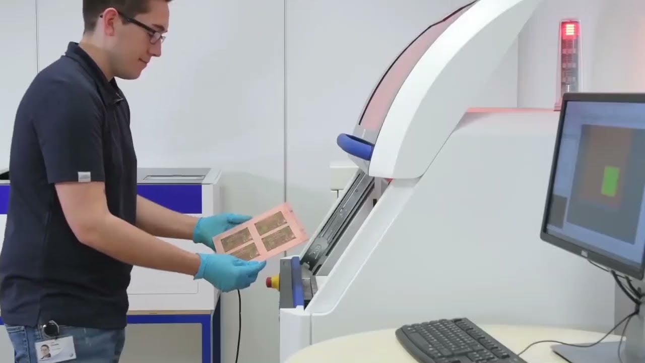
The need for a multilayer PCB is evident. It can handle higher complexity on a smaller PCB footprint, ensuring better signal integrity, including high-speed communication, and a more efficient power supply.
Rapid PCB prototyping equipment addresses all steps, processing inner and outer layers, blind, buried, and through-hole drilling, and plating with LPKF ProtoLaser, Multi-Press S4, and Contac S4.
For more understanding of what happens during the pressing process check: • Flexible Multilayer PCB – What Really...
Multilayer boards on all laminated materials, such as copper-clad FR4, ceramic or PTFE-filled RF materials, or copper-coated foil materials, are possible: https://bit.ly/3VUpyR9
Find out more about in-house Multilayer processing in LPKF´s virtual showroom LPKF Product Showroom: https://bit.ly/3LfrrTG
Повторяем попытку...
Доступные форматы для скачивания:
Скачать видео
-
Информация по загрузке:


![Как сжимаются изображения? [46 МБ ↘↘ 4,07 МБ] JPEG в деталях](https://image.4k-video.ru/id-video/Kv1Hiv3ox8I)


