Conductor, Semiconductor, Insulator || Types of Semiconductor || Basic Electronics
Автор: ElectroTech CC
Загружено: 2020-05-21
Просмотров: 496
Описание:
#ElectroTechCC #Typesofsemiconductor
Conductor, Semiconductor, Instulator
Types of Semiconductor
Basic Electronics
Previous video on
Atomic Bonds || Valence & Conduction Bands || Solid State Physics ||Basic Electronics
Click Here: • Atomic Bonds || Valence & Conduction Bands...
Conductor, Semiconductors and insulators:
• Electrical conduction properties of different elements and compounds can be explained in terms of the electrons having energies in the valence and conduction bands
• (a) Insulators:
o Materials in which valence electrons are bound very tightly to their parent atoms thus requiring very large electric field to remove from attraction of their nucleus.
o Insulators have full valence band, an empty conduction band, and a large energy gap between them
o Increase in temperature enables some electrons to go to the conduction band which fact accounts for the negative temperature coefficient of resistance of insulators
• (B)Conductors:
o Conducting materials are those in which plenty of free electrons are available for electric conduction
o Electrical conductors have overlapping valence and conduction bands, absence of forbidden gap in good conductors
o Available large number of conduction electrons
o Total current in such conductors is simply a flow of electrons
• (C)Semiconductors:
o Material whose electrical properties lie in between those of insulators and good conductors
o For example, Ge and Si
o Semiconductors can be defined as those materials which at room temperature have
Partially filled conduction band
Partially filled valence band and
A very narrow energy gap
o At 0’ K there are no electrons in the conduction band of semiconductors and their valence band is completely filled
o At absolute zero temperature, a piece of Ge or Si acts like a perfect insulator
o With increase in temperature width of the forbidden energy band is decreased so that some of the electrons are liberated into the conduction band – conductivity of semiconductor increases with temperature – negative temperature coefficient
Types of Semiconductors:
• Intrinsic or pure semiconductor
• Extrinsic or impure semiconductor
o N-type
o P-type
• Intrinsic or Pure Semiconductor
o Pure form of semiconductor
o For example, Pure germanium and silicon which have forbidden energy gaps of 0.72 eV to 1.1 eV respectively
o The energy gap is so small that even at ordinary room temperature, there are many electrons which possess sufficient energy to jump across the small energy gap form the valence to the conduction band, a positive charged hole is created in the valence band
o When electrical field is applied to an intrinsic semiconductor at temperature greater than 0’ K, conduction electrons move to the anode and holes in the valence band move to the cathode
o Semiconductor current consists of movement of electrons and holes in opposite directions in the conduction and valence bands
o Intrinsic semiconductor may be defined as one in which the number of conduction electrons is equal to the number of holes
• Extrinsic Semiconductor:
o Those intrinsic semiconductors to which some suitable impurity or doping agent has been added in extremely small amount (1 part in 108)
o Pentavalent atoms having five valence electrons (Antimony, Arsenic, Phosphorus) or tetravalent atoms having three valence electrons (Gallium, Idiom, Aluminium, Boron) used as a doping agent
o Pentavalent atom is known as donor atom because it donates or contributes one electron to the conduction band of pure Ge.
o Trivalent atom is known as acceptor atom because it accepts one electron from the germanium atom
• Depending on the type of doping material used, it can be further classified into two classes:
o N-type semiconductor
o P-type semiconductor
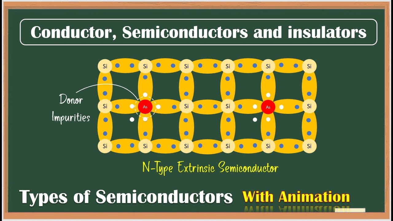
• N-Type Extrinsic Semiconductor:
o This type of semiconductor is obtained when a pentavalent material like antimony (Sb) is added to pure germanium crystal
o Each antimony atom forms covalent bonds with the surrounding four germanium atoms with the help of four of its five electrons
o The 5th electron is superfluous and is loosely bound to the antimony atom
o It can be easily excited from the valence band to the conduction band by application of electrical field or increase in its thermal energy
o Every antimony atom introduced into the germanium lattice contributes one conduction electron without creating a positive hole
o Antimony is called donor impurity and makes the pure Ge an N-type extrinsic semiconductor
• P-Type Extrinsic Semiconductor:
o When trivalent impurity like boron(B) are added to a pure Ge crystal
o Three valence electrons of boron atom form covalent bonds with four surrounding Ge atoms, but one bond is left incomplete and gives rise to a hole
#ElectronicsandCommunicationEngineering
#ElectroncisComponents
#BasicElectronics
#EngineeringPhysics
#GTU
#DiplomaEngineering
#12stScience
My channel publishes videos that focus on Electronics Concept. If that sounds like it could be helpful for you, please join me!
Повторяем попытку...
Доступные форматы для скачивания:
Скачать видео
-
Информация по загрузке:


![Пожалуй, главное заблуждение об электричестве [Veritasium]](https://image.4k-video.ru/id-video/6Hv2GLtnf2c)


