Siltronic Animated Wafer Production Process
Автор: Siltronic AG
Загружено: 2021-02-25
Просмотров: 29078
Описание:
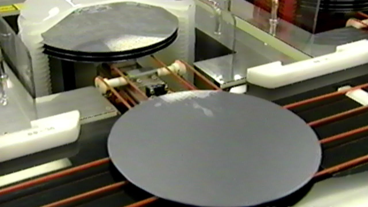
HOW TO MAKE A SILICON WAFER
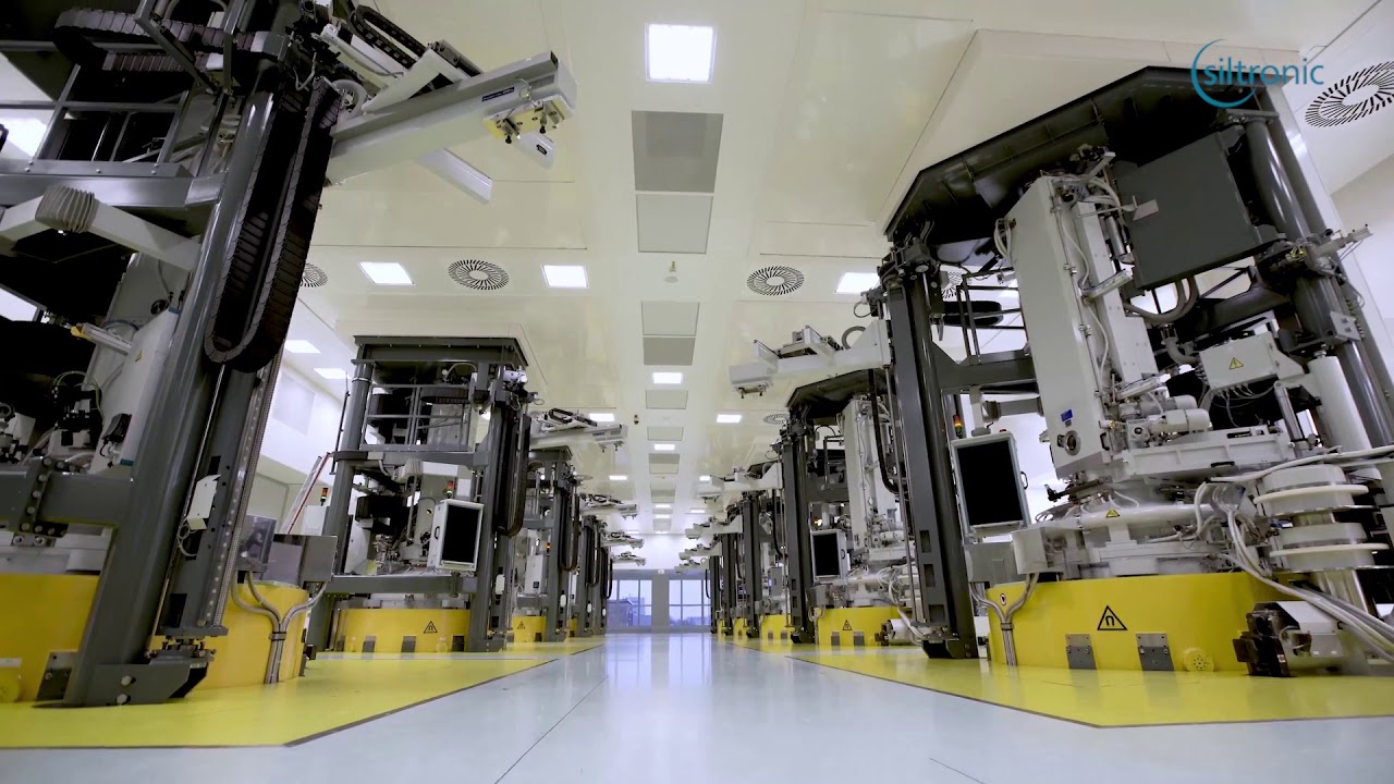
A wafer is a slice of silicon roughly 1 millimeter thick that has an extremely flat surface thanks to procedures that are technically very demanding. The subsequent use determines which crystal growing procedure should be employed. In the Czochralski process, for example, the polycrystalline silicon is melted and a pencil-thin seed crystal is dipped into the molten silicon. The seed crystal is then rotated and slowly pulled upwards. A very heavy colossus, a monocrystal, results. It is possible to select the monocrystal’s electrical characteristics by adding small units of high-purity dopants. The crystals are doped in accordance with the customer specifications and then polished and cut into slices. After various additional production steps, the customer receives its specified wafers in special packaging, which allows the customer to use the wafer immediately in its production line.
Повторяем попытку...

Доступные форматы для скачивания:
Скачать видео
-
Информация по загрузке:


![[공정 소개] SK hynix Wafer Fabrication](https://imager.clipsaver.ru/AcDn4bvW5IU/max.jpg)