Focusing on Manufacturing Equipment for Semiconductors to Support Our Future (Canon Official)
Автор: Canon
Загружено: 2025-07-29
Просмотров: 752
Описание:
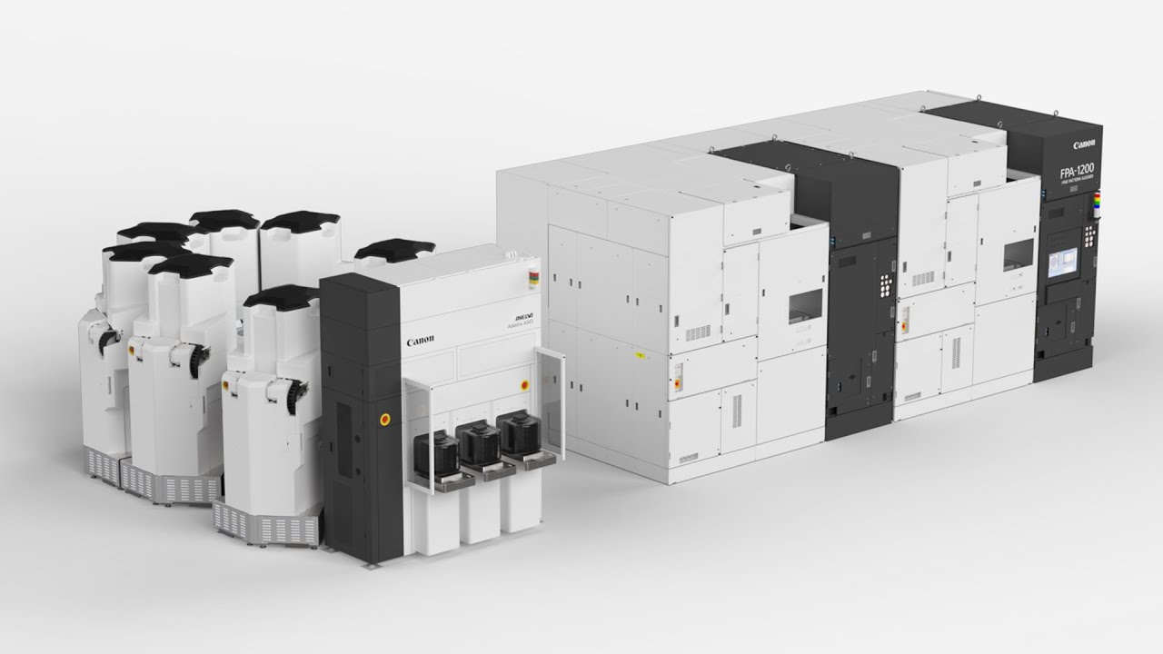
With the growing diversification of semiconductor devices in recent years, the manufacturing processes have become increasingly complex, and there is also a need to respond flexibly to customer needs. Using the example of Adastra, a new platform of equipment with film deposition technology developed by CANON ANELVA, this seminar will introduce the challenges encountered when designing equipment while also venturing into the domains of exterior and usability.
We will also introduce the development story of the FPA-1200NZ2C, the world’s first nanoimprint lithography semiconductor manufacturing equipment for mass production that applies the principle of stamping to the semiconductor manufacturing process, thus achieving even finer semiconductor circuit patterns and significantly reducing environmental impact.
0:00 Opening
3:06 The FPA-1200NZ2C Development Story
11:15 Adastra
26:20 Ending
■Canon YouTube channel
Subscribe to the official Canon YouTube channel
/ @canonchannel
■Canon Imaging Plaza
Subscribe to the official Canon Imaging Plaza YouTube channel
/ @canonimagingplaza
Official Canon website
https://global.canon/
#CanonOfficial #MeetupCanonDesign #CanonDesign #Productdesign #Usability #Semiconductor #ManufacturingEquipment #Ecofriendliness #Adastra #nanoimprint #nanoimprintlithography #FPA1200NZ2C #GoodDesignGoldAward #GoldAward #goldprize
#industrial #semiconductor
Повторяем попытку...
Доступные форматы для скачивания:
Скачать видео
-
Информация по загрузке:


![Как устроен эскалатор? [Veritasium]](https://image.4k-video.ru/id-video/MIlDmkGn4Qc)


