Скачать
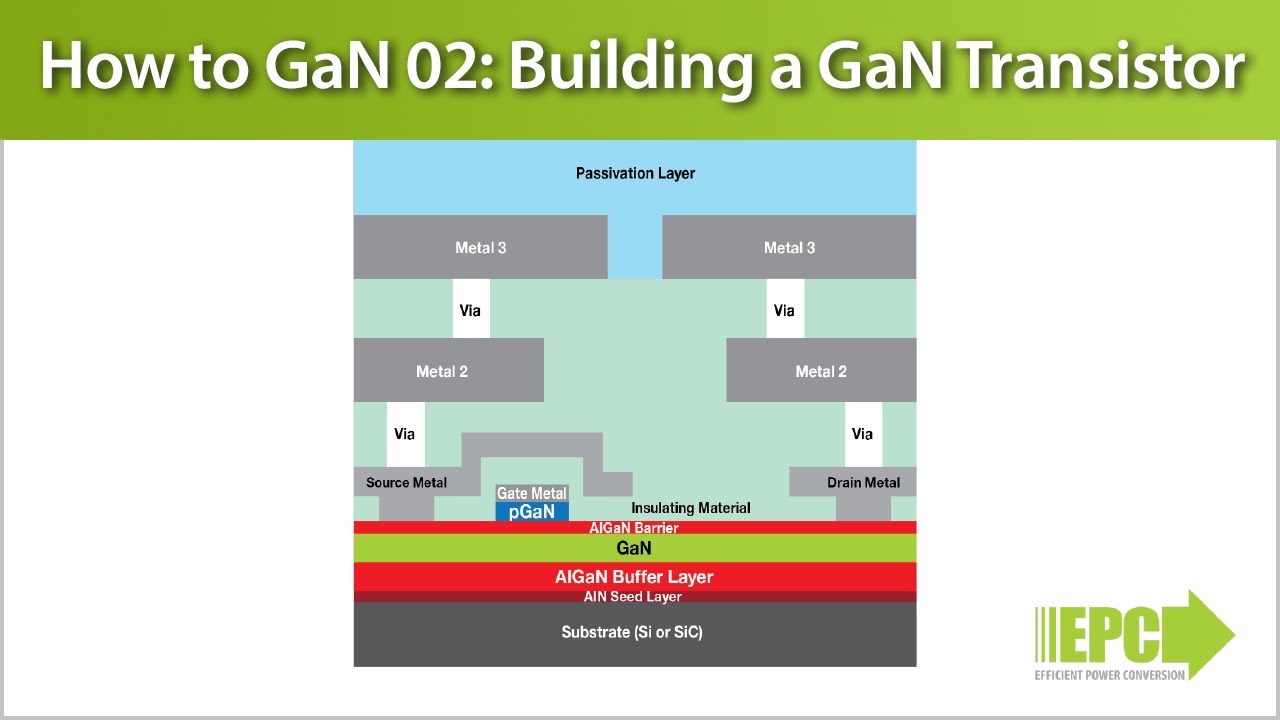
How to GaN 02 – Building a Gallium Nitride (GaN) Transistor
Автор: EPC Corporation
Загружено: 2020-03-29
Просмотров: 22215
Описание:
This video will provide a basic understanding of how to build a GaN transistor utilizing a low cost substrate and a large, well-developed infrastructure.
0:00 Start
0:21 Steps to building a GaN transistor
0:45 Substrate material selection
2:28 Growing the heteroepitaxy
3:47 Wafer processing
5:02 Cross-section of an eGaN FET
5:36 Chip-scale packaging
6:56 Completed GaN transistor
Не удается загрузить Youtube-плеер. Проверьте блокировку Youtube в вашей сети.
Повторяем попытку...
Повторяем попытку...
Доступные форматы для скачивания:
Скачать видео
-
Информация по загрузке: