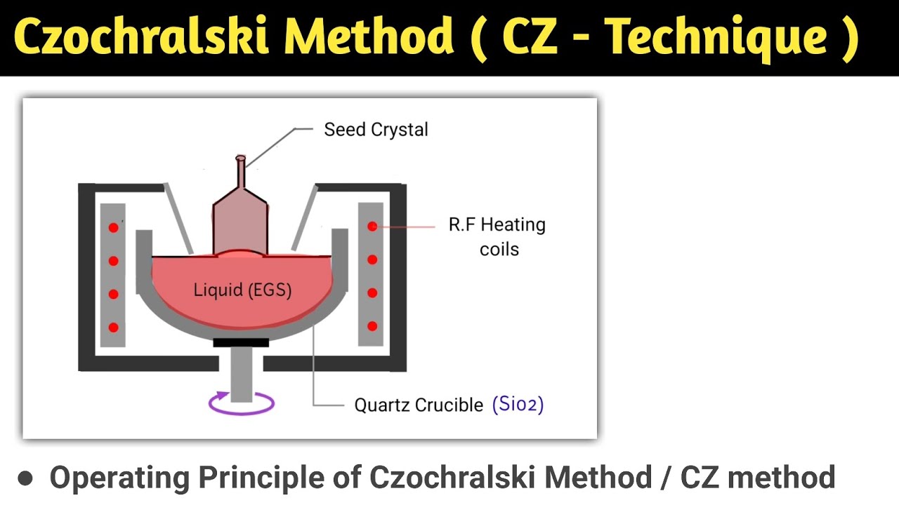
Lec-6 | Epitaxial growth and Lattice matching | Technology of Semiconductors
Автор: Udta Engineer
Загружено: 2018-06-13
Просмотров: 26002
Описание:
This lecture deals with Epitaxial growth and lattice matching.
Hi Friends,
I welcome you to the world of Electrocombot and Udta engineer.
Earlier the name of my channel was " ElectroComBot " but I recently changed the name to Udta engineer as it perfectly matches the theme of my channel.
This channel is all about exploring the fundamentals of engineering and simultaneously enhancing the living experience by making travel-related videos. I always feel that going for a trip is always better than reading 100 books as it provides a completely different horizon and way of living which can never be grasped from books.
In this channel, you can find videos related to engineering where I have tried to simplify the concepts and if you get bored after studying then you can switch to travel-related videos to refresh yourself.
So stay tuned !!!!
Повторяем попытку...

Доступные форматы для скачивания:
Скачать видео
-
Информация по загрузке: