Correct Steps in the Manufacturing Process of Multilayer PCB Circuit
Автор: SMTSKY
Загружено: 2026-02-01
Просмотров: 2
Описание:
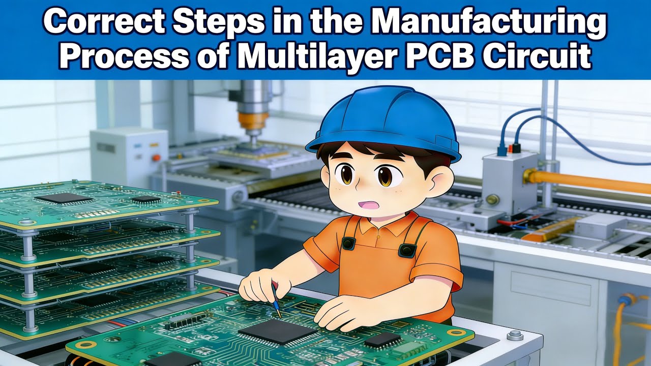
Hello everyone, today l'm gonna elaborate the correct steps in the
manufacturing process of a multi layer pcb . This video demonstrates
the pcb manufacturing process, starting with design and layout using
software, showing how it's made . lt then shows the transfer of the
design to copper clad boards via photolithography and the subsequent
drilling and etching processes, making it a great guide for pcb for
beginners . Finally, the video illustrates the soldering of components
onto the finished circuit board, helping you understand how the pcb
explained works.
Steps Covered:
1.Designing the PCB Circuit
2.Printing the PCB Design onto Copper
3.Etching to Remove Unwanted Copper
4.Drilling Holes for Vias and Components
5.Laminating and Bonding the Layers
6.Applying Solder Mask & Silkscreen
7.Final Inspection and Testing
📩 Want help solving SMT defects in your line?
We support global SMT & electronics manufacturing projects, including:
• SMT process analysis & defect troubleshooting
• PCB assembly risk evaluation
• Equipment / feeder / consumable selection support
• Manufacturing-oriented technical consulting
👉 Contact us for technical discussion or cooperation:
📧 Email: [email protected]
💬 WhatsApp: +86 13798971171
🌐 Website: www.smtsky.com
Повторяем попытку...
Доступные форматы для скачивания:
Скачать видео
-
Информация по загрузке: