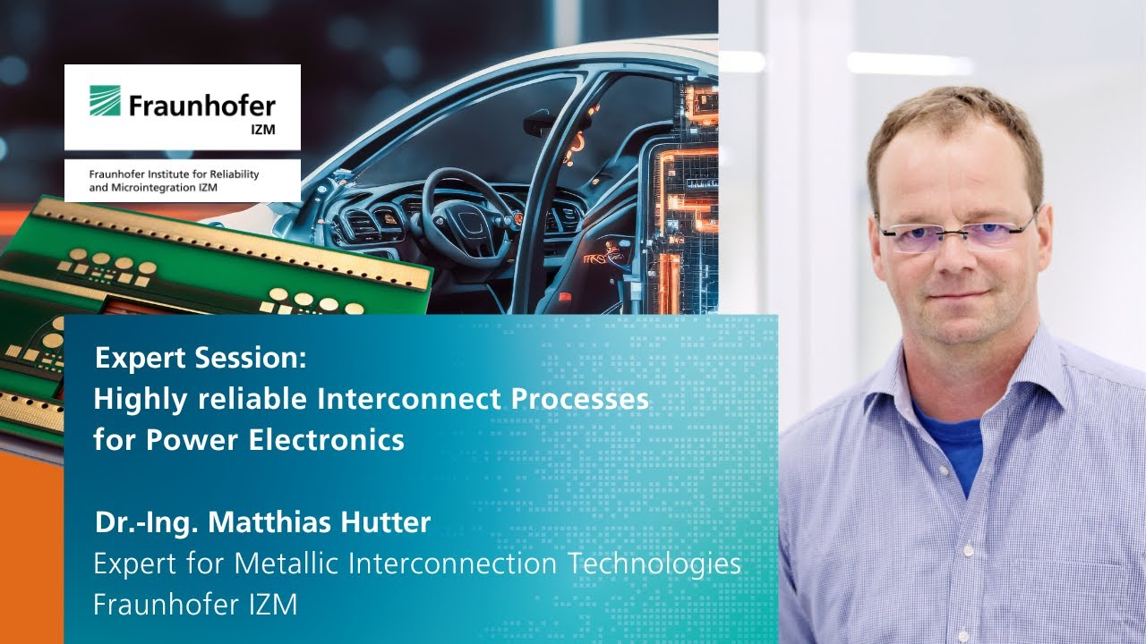
Expert Session: Concepts for Power Electronics – PCB Embedding for SiC and GaN Semiconductors
Автор: Fraunhofer IZM
Загружено: 2024-03-26
Просмотров: 1388
Описание:
#4 Expert Session of Series »Powering the Future - Innovative Technologies for Power Electronics Modules with SiC and GaN Semiconductors«
Speaker: Lars Böttcher, expert for Embedding and Substrate Technology, Fraunhofer IZM
Power modules equipped with wide band gap semiconductors like SiC and GaN are attracting increasing attention, due to the superior functionality of these materials. Especially for automotive, aerospace and energy grid applications, a large market potential is expected. Today’s power electronics modules typically consist of a ceramic substrate (DBC or AMB), carrying the power semiconductors, which are soldered and wire bonded for interconnection. Driver circuits and controllers have to be mounted to a separate substrate, which has to be connected to the DBC/AMB by wires or pins. The mechanical integration of the whole system requires a bulky housing. The electrical performance for devices with the potential for fast switching are limited by these module concepts and it’s interconnections.
Major aims in system optimization are the reduction of DC voltage link inductance, optimization of heat dissipation and an overall miniaturization and robustness of modules. Consequently, the shortening of interconnect length, the integration of thermal dissipation structures and a compact three-dimensional build-up of systems are of highest interest.
Embedding of SiC or GaN allows a significant size reduction, improved electrical and thermal performance and a high degree of reliability of such modules.
For the embedding of SiC bare dies, the dies are assembled to a suitable substrate by Ag sintering. Printed circuit board technologies are used to embed the devices into a polymer matrix by multilayer vacuum lamination, using epoxy prepreg material. Direct copper connections to the embedded SiC die are realized by laser via formation and electrolytic copper plating. Thick copper technologies could be implemented if needed for high currents and thermal management. If required, multiple wiring layers can be created, using PCB manufacturing processes
The session will give a general overview about innovative power module technologies and will explain the embedding of power semiconductors in detail. Here it will address all most relevant points, like the demands on the semiconductor, the thermal and electrical considerations as well as the demands on the used materials. The technology approach will be described in detail and different module examples will be introduced and discussed.
To address the integration of the required driver circuits and controllers, the idea of modularization such electronics systems will also be introduced.
Picture: Limitless Visions - adobe.stock.com and Fraunhofer IZM
#reliability #pcb #siliconcarbide #powerelectronics #fraunhoferizm #microelectronics
___________
Official website: https://www.izm.fraunhofer.de/
Follow us on LinkedIn: / 489228
Follow us on Twitter: / fraunhofer_izm
Follow us on Instagram: https://www.instagram.com/fraunhofer_...
Subscribe to our blog RealIZM: https://blog.izm.fraunhofer.de/
Повторяем попытку...
Доступные форматы для скачивания:
Скачать видео
-
Информация по загрузке: