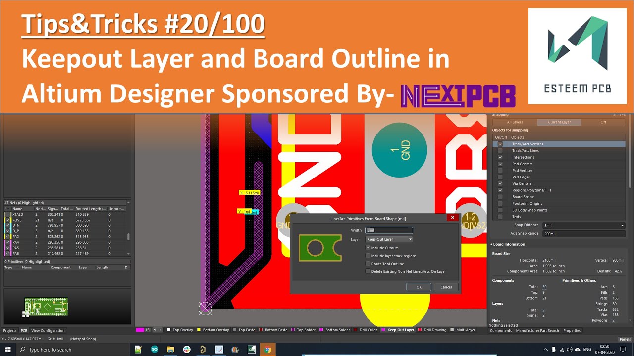
Altium Designer Tips #20: Create Keepout Layer and Board Outline in Altium
Автор: EsteemPCB Academy
Загружено: 2020-04-09
Просмотров: 18407
Описание:
Free!!! $5 Registration Link: https://www.nextpcb.com/register?code...
Gifts link: https://docs.google.com/forms/d/e/1FA...
#FreePCBsbyNextPCB #SubscribeForUpadates
$0 for IATF Certification PCB Prototype (24 hours lead time): https://www.nextpcb.com?code=esteemyo...
Get 10% Off For Your PCB & PCB Assembly Order:
https://www.nextpcb.com/activity_ther...
Learn more about PCB assembly: https://www.nextpcb.com/pcb-assembly-...
NextPCB is one of the most experienced PCB manufacturers in China and has 15 years of experience with UL & ISO9001 & ISO4001 Certified to ensure the PCB quality of your project.
*****************************************************************************************************
In this series, we'll be going to discuss 100 Altium Designer Tips and Altium designer tools by using that designing will be very easy. Enjoy Altium designer Tutorials How to #Create #Keepout #Layer and #Board #Outline in #Altium #Designer.
******************************************************************************************************
I Need to Start Writing Things Down by Chris Zabriskie is licensed under a Creative Commons Attribution license (https://creativecommons.org/licenses/...)
Source: http://chriszabriskie.com/darkglow/
Artist: http://chriszabriskie.com/
The Copyright Laws of the United States recognizes a “fair use” of copyrighted content. Section 107 of the U.S. Copyright Act states:
“Notwithstanding the provisions of sections 106 and 106A, the fair use of a copyrighted work, including such use by reproduction in copies or phonorecords or by any other means specified by that section, for purposes such as criticism, comment, news reporting, teaching (including multiple copies for classroom use), scholarship, or research, is not an infringement of copyright.”
This video and our YouTube channel, in general, may contain certain copyrighted works that were not specifically authorized to be used by the copyright holder(s), but which we believe in good faith are protected by federal law and the fair use doctrine for one or more of the reasons noted above.
If you have any specific concerns about this video or our position on the fair use defence, please contact us at "[email protected]" so we can discuss amicably.
Thank you.
Повторяем попытку...
Доступные форматы для скачивания:
Скачать видео
-
Информация по загрузке:


