ycliper

Популярное

Музыка Кино и Анимация Автомобили Животные Спорт Путешествия Игры Юмор

Интересные видео

2025 Сериалы Трейлеры Новости Как сделать Видеоуроки Diy своими руками

Топ запросов

смотреть а4 schoolboy runaway турецкий сериал смотреть мультфильмы эдисон
Скачать

Via Stitching and Shielding | Altium Designer 17 Advanced | Module 11

Автор: Altium Academy

Загружено: 2019-09-19

Просмотров: 36382

Описание: In this Altium Designer 17 Advanced PCB training course module, you will learn:
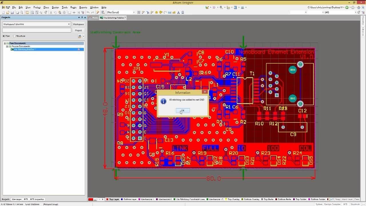
How to add "stitching vias" to areas of the board and nets like GND or power.
How to add shielding vias (also known as "via fences") to critical high speed or RF nets.
How to control the spacing, pattern, and via styles of stitching and shielding vias.
How to remove selected vias from shielding or stitching pattern groups.
How to add shielding surrounding an entire net class.

Download all the example files associated with this training here: http://chilp.it/4b16caf
Design PCBs with a Free Trial of Altium Designer Here:

Download CircuitMaker Here: https://www.altium.com/circuitmaker/d...

The Altium Academy is an online experience created to bring modern education to PCB Designers and Engineers all across the world. Here you can access a vast library of free training and educational content covering everything from basic design to advanced principles and step-by-step walkthroughs. Join industry legends as they share their career knowledge, review real-life design projects, or learn how to leverage one of Altium's leading design tools. No matter your level of experience, the Altium Academy can help you become a better Designer and Engineer!

About Altium LLC
Altium LLC (ASX:ALU), a global software company based in San Diego, California, is accelerating the pace of innovation through electronics. From individual inventors to multinational corporations, more PCB designers and engineers choose Altium software to design and realize electronics-based products.


#Altium #PCBdesign

~-~~-~~~-~~-~
Check Out Our Latest Video: "How to Draw Antipads"
   • How to Draw Antipads - Complete Tutorial  
~-~~-~~~-~~-~

Не удается загрузить Youtube-плеер. Проверьте блокировку Youtube в вашей сети.
Повторяем попытку...
Via Stitching and Shielding | Altium Designer 17 Advanced | Module 11

Поделиться в:

Доступные форматы для скачивания:

Скачать видео

  • Информация по загрузке:

Скачать аудио

Похожие видео

Differential Pairs | Altium Designer 17 Advanced | Module 12

Differential Pairs | Altium Designer 17 Advanced | Module 12

How GND VIAs Improve Your PCB Layout

How GND VIAs Improve Your PCB Layout

10 Killer Tips and Tricks for Altium Designer 23

10 Killer Tips and Tricks for Altium Designer 23

PCB Component Placement Webinar

PCB Component Placement Webinar

Efficient PCB Routing Using Gloss and Retrace Tools

Efficient PCB Routing Using Gloss and Retrace Tools

Top 5 Beginner PCB Design Mistakes (and how to fix them)

Top 5 Beginner PCB Design Mistakes (and how to fix them)

Vias and Their Aspect Ratios | PCB Routing

Vias and Their Aspect Ratios | PCB Routing

(Sponsored) 2-Layer PCB Design Tips - Phil's Lab #137

(Sponsored) 2-Layer PCB Design Tips - Phil's Lab #137

Floods, Planes and Polygons for Ground and Power | Altium Designer 17 Essentials | Module 24

Floods, Planes and Polygons for Ground and Power | Altium Designer 17 Essentials | Module 24

Сшивание с помощью Deep Dive | Разводка печатной платы

Сшивание с помощью Deep Dive | Разводка печатной платы

(Sponsored) PCB Vias 101 - Phil's Lab #77

(Sponsored) PCB Vias 101 - Phil's Lab #77

(Sponsored) PCB Stack-Up and Build-Up - Phil's Lab #56

(Sponsored) PCB Stack-Up and Build-Up - Phil's Lab #56

Руководство по ESP32 2024 | Выбор и использование платы ESP32

Руководство по ESP32 2024 | Выбор и использование платы ESP32

Два инженера соревнуются в разработке печатной платы всего за час! Кто победит?

Два инженера соревнуются в разработке печатной платы всего за час! Кто победит?

Орешник: новые и старые сведения

Орешник: новые и старые сведения

How To Define and Place Vias in Altium Designer?

How To Define and Place Vias in Altium Designer?

Где начало СХЕМЫ? Понимаем, читаем, изучаем схемы. Понятное объяснение!

Где начало СХЕМЫ? Понимаем, читаем, изучаем схемы. Понятное объяснение!

To Pour or Not To Pour | Copper Pour in PCB Design

To Pour or Not To Pour | Copper Pour in PCB Design

Do you also make these mistakes in PCB Layout?

Do you also make these mistakes in PCB Layout?

PCB Stack-up and Controlled Impedance in Altium Designer

PCB Stack-up and Controlled Impedance in Altium Designer

© 2025 ycliper. Все права защищены.


  • Контакты
  • О нас
  • Политика конфиденциальности


Контакты для правообладателей: [email protected]