Скачать
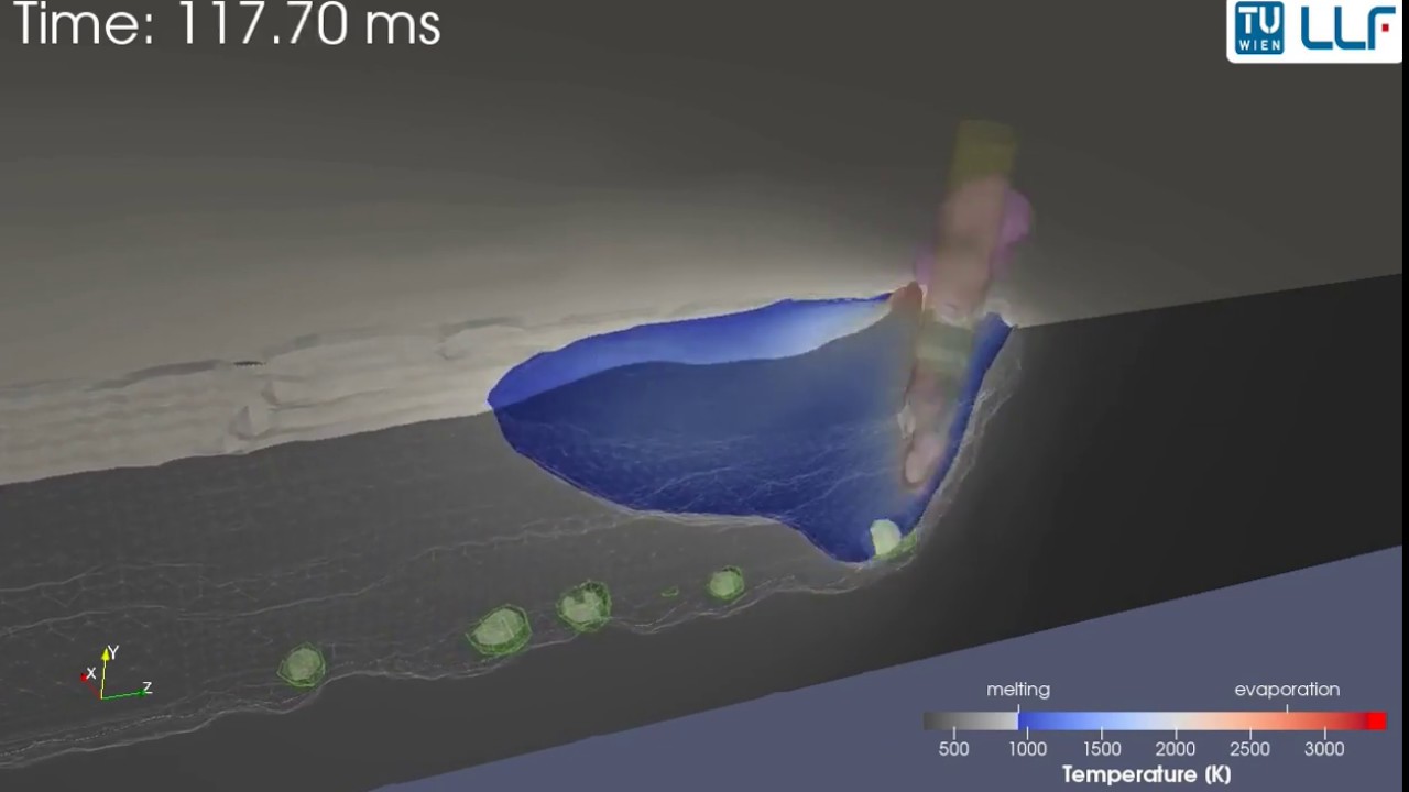
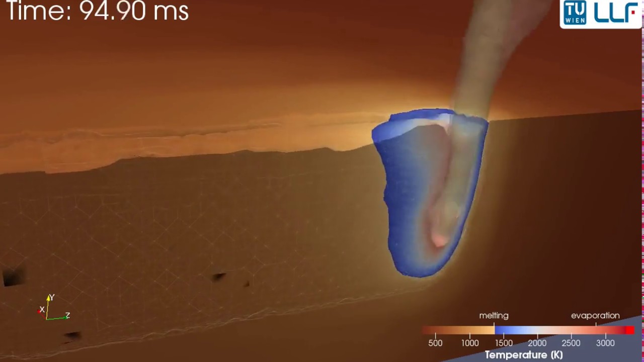
Laser scribing of Si wafer (low power)
Автор: Laser Assisted Manufacturing, TU Wien
Загружено: 2016-10-21
Просмотров: 1477
Описание:
Ablation of a silicon substrate with laser pulses. This is an old feasibility study (not validated!). Simulation carried out at the Research Unit of Photonic Technologies (Vienna University of Technology).
http://llf.ift.tuwien.ac.at
Process parameters:
λ: 355nm,
spot size: 10µm,
pulse energy: 10µJ,
pulse length: 50ns,
pulse frequency: 250kHZ,
path: 8 pulses,
scanning speed: 1670mm/s
The simulation environment used was OpenFOAM (https://openfoam.org/).
Не удается загрузить Youtube-плеер. Проверьте блокировку Youtube в вашей сети.
Повторяем попытку...
Повторяем попытку...

Доступные форматы для скачивания:
Скачать видео
-
Информация по загрузке:


![Почему реактивный двигатель не плавится? [Veritasium]](https://imager.clipsaver.ru/F6UB0V2Fct4/max.jpg)