PCB Design Tutorial PART#02: ESP32 Double-Layer PCB Layout & Routing with USB-C | Full Walkthrough
Автор: Embedded Minds
Загружено: 2025-11-11
Просмотров: 65
Описание:
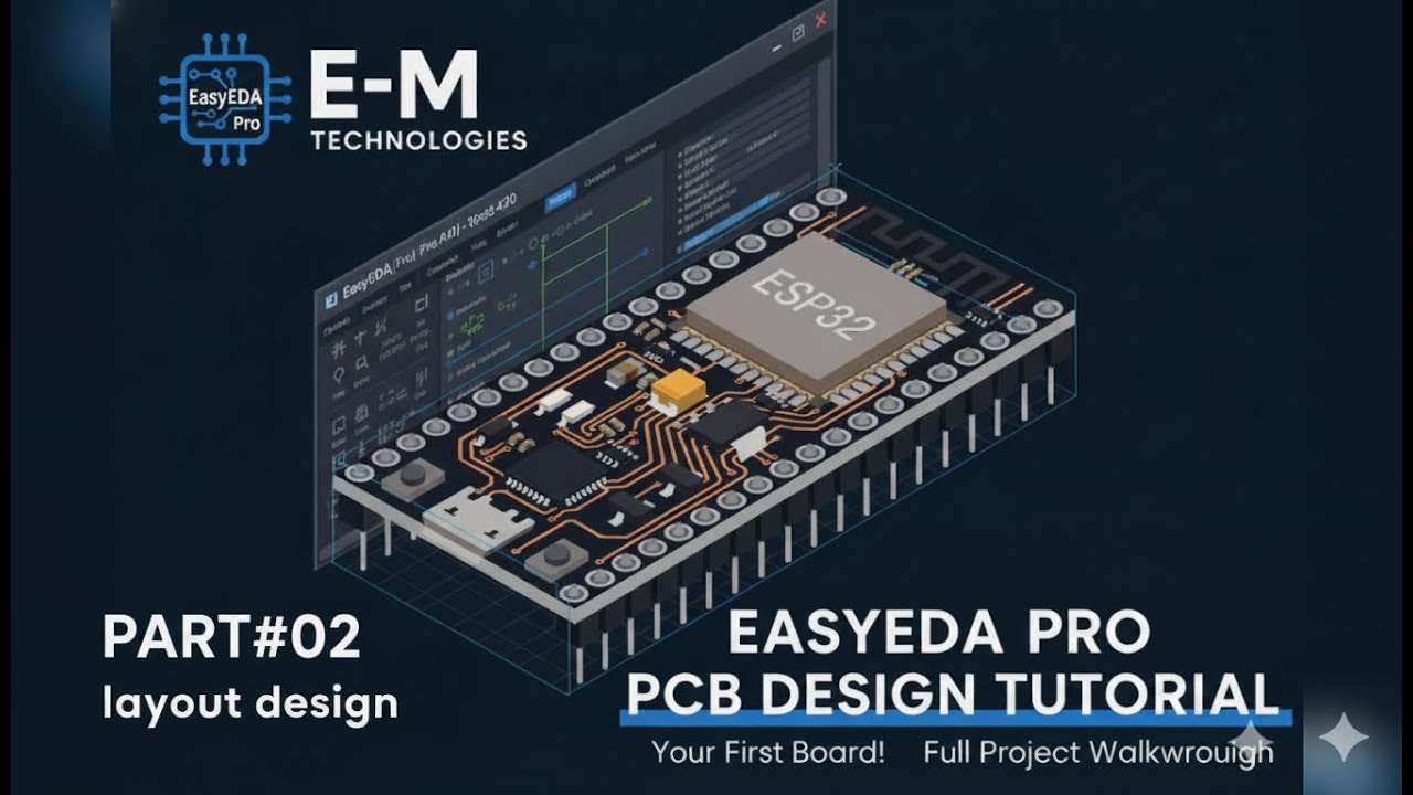
PART#02: ESP32 PCB Layout & Routing (Double-Layer)
Welcome to the second installment of our professional EasyEDA Pro PCB Design series! In this tutorial, we transition the schematic developed in Part 1 into a manufacturable double-layer PCB for a custom ESP32 development board.
This video provides a complete, step-by-step walkthrough covering the critical aspects of physical board design:
Key Topics Covered:
Component Placement: Strategic placement of the ESP32 module, supporting components, and critical USB Type-C circuitry for optimal signal integrity and thermal performance.
Layer Stackup: Configuring the double-layer board structure and defining design rules within EasyEDA Pro.
USB Type-C Implementation: Integrating the USB-C connector for both reliable power delivery and the necessary programming/data interface for the ESP32.
Advanced Routing: A full demonstration of routing a complex double-layer board, including handling differential pairs, power planes, and ensuring proper trace width for low-power consumption.
Mastering PCB layout is essential for reliable electronic products. By the end of this video, you will have a fully routed, production-ready ESP32 design file.
---
🔗 Watch PART#01: ESP32 Schematic Design Here: • Design Your First ESP32 PCB in #easyeda P...
If this video helped you, please Like, Subscribe, and turn on Notifications for more professional hardware design tutorials!
#easyeda #pcb #esp32
Повторяем попытку...
Доступные форматы для скачивания:
Скачать видео
-
Информация по загрузке:


